
1
Date:5/25/04
SP6200/6201 100/200mA CMOS LDO Regulator
© Copyright 2004 Sipex Corporation
Tiny DFN Package (2mmX3mm)
Low Dropout Voltage: 160mV @ 100mA
High Output Voltage Accuracy: 2%
Ultra Low Shutdown Current: 1
µ
A Max
Ultra Low GND Current:
∑ 200
µ
A @ 200mA Load
∑ 28
µ
A @ 100
µ
A Load
Extremely Tight Load and Line Regulation
Current and Thermal Limiting
RESET Output (V
OUT
good)
Logic-Controlled Electronic Enable
Unconditionally Stable with 1
µ
F Ceramic
Fixed Outputs:
∑ 1.5V, 1.8V, 2.5V, 2.7V, 2.85V, 3.0V, 3.3V, 3.5V, 5V
Adjustable Output Available
Micropower, 100mA and 200mA CMOS LDO Regulators
SP6200/6201
DESCRIPTION
Cellular Telephones
Laptop, Notebooks and Palmtop Computers
Battery-Powered Equipment
Consumer/ Personal Electronics
SMPS Post-Regulator
DC-to-DC Modules
Medical Devices
Data Cable
Pagers
FEATURES
APPLICATIONS
Æ
Fixed Output Voltage
The SP6200 and SP6201 are CMOS LDOs designed to meet a broad range of applications that require accuracy, speed
and ease of use. These LDOs offer extremely low quiescent current which only increases slightly under load, thus
providing advantages in ground current performance over bipolar LDOs. The LDOs handle an extremely wide load range
and guarantee stability with a 1
µ
F ceramic output capacitor. They have excellent low frequency PSRR, not found in other
CMOS LDOs and thus offer exceptional Line Regulation. High frequency PSRR is better than 40dB up to 400kHz. Load
Regulation is excellent and temperature stability is comparable to bipolar LDOs. An enable feature is provided on all
versions.
The SP6200/6201 is available in fixed and adjustable output voltage versions in tiny DFN and small SOT-23-5 packages.
A V
OUT
good indicator is provided on all fixed output versions.
3
2
1
5
4
EN
SP6200
SP6201
V
OUT
C
OUT
=
1
µ
F
V
IN
Enable
Shutdown
RSN
EN (pin 3) may be connected
directly to IN (pin 1).
(V
OUT
good)
C
IN
=
1
µ
F
470k
TYPICAL APPLICATION CIRCUIT
RESET
EN
NC
VIN
VOUT
NC
GND
SP6201
8 Pin DFN
NC
1
2
3
4
5
6
7
8
Now Available in Lead Free Packaging
2
Date:5/25/04
SP6200/6201 100/200mA CMOS LDO Regulator
© Copyright 2004 Sipex Corporation
ELECTRICAL CHARACTERISTICS
ABSOLUTE MAXIMUM RATINGS, NOTE 1
These are stress ratings only and functional operation of
the device at these ratings or any other above those
indicated in the operation sections of the specifications
below is not implied. Exposure to absolute maximum
rating conditions for extended periods of time may affect
reliability.
Supply Input Voltage (V
IN
) ............................. -2V to 7V
Output Voltage (V
OUT
) ......................... -0.6 to (V
IN
+1V)
Enable Input Voltage (V
EN
) ............................ -2V to 7V
Power Dissipation (P
D
) .......... Internally Limited, Note 3
Lead Temperature (soldering 5s) ....................... 260
∞
C
Storage Temperature ........................ -65∞C to +150∞C
OPERATING RATINGS, NOTE 2
Input Voltage (V
IN
)..................................+2.5V to +6V
Enable Input Voltage (V
EN
)..........................0V to +6V
Junction Temperature (T
J
)................-40∞C to +125∞C
Thermal Resistance (See Note 3):
SOT-23-5 (
JA
)...................................................90∞C/W
8 Pin DFN (
JA
)............................................ .....59∞C/W
(See Note 3)
V
IN
= V
OUT
+1V, V
O
= 5V for ADJ, I
L
= 100
µ
A, C
IN
= 1.0
µ
F, C
OUT
= 1.0
µ
F, T
J
= 25
∞
C , unless otherwise specified. The
denotes the specifications
which apply over the full operating temperature range, unless otherwise specified.
PARAMETER
MIN
TYP
MAX
UNIT
CONDITIONS
Output Voltage Accuracy, (V
O
)
-2
2
%
Variation from specified V
OUT
-3
3
%
Reference Voltage
1.213
1.250
1.287
V
Adjustable version only
Output Voltage Temperature
60
ppm/
∞
C
Coefficient, Note 4, (
V
O
/
T)
Minimum Supply Voltage
2.50
2.70
V
I
L
= 100
µ
A
2.55
2.80
V
I
L
= 50mA
2.70
2.95
V
I
L
= 100mA
3.00
3.50
V
I
C
= 200mA
Line Regulation, (
V
O
/ V
IN
)
0.03
0.2
%/ V
V
IN
= (V
OUT
+ 1V) to 6V
Load Regulation, Note 5, (
V
O /
V
O
)
0.07
0.25
%
I
L
= 0.1mA to 100mA, SP6200
0.14
0.50
%
I
L
= 0.1mA to 200mA, SP6201
SP6200-1.5V & 1.8 Load Regulation
0.3
1
%
I
L
= 0.1mA to 100mA, V
IN
= 2.95V
SP6201-1.5V & 1.8 Load Regulation
0.3
1
%
I
L
= 0.1mA to 200mA, V
IN
= 3.5V
Dropout Voltage, Note 6, (V
IN
≠ V
O
)
0.2
4
mV
I
L
= 100
µ
A
(Not applicable to voltage options below
7
mV
2.7V)
70
120
mV
I
L
= 50mA
160
mV
160
250
mV
I
L
= 100mA
300
mV
320
400
mV
I
L
= 200mA, SP6201 Only
500
mV
Shutdown Quiescent Current, (I
GND
)
0.01
1
µ
A
V
EN
0.4V
Ground Pin Current, Note 7, (I
GND
)
28
40
µ
A
V
EN
2.0V, I
L
= 100
µ
A
45
µ
A
110
200
µ
A
V
EN
2.0V, I
L
= 100mA, SP6200
250
µ
A
only (for 1.5 & 1.8, V
IN
= 2.95)
200
400
µ
A
V
EN
2.0V, I
L
= 200mA, SP6201
500
µ
A
Only (for 1.5 & 1.8, V
IN
= 3.5)
Power Supply Rejection Ratio,
78
Frequency =100Hz, IL =10mA
(PSRR)
40
dB
Frequency = 400Hz, IL=10mA
Current Limit, (I
CL
)
100
140
200
mA
SP6200
300
420
600
mA
SP6201
Thermal Limit
162
∞
C
Turns On
147
∞
C
Turns Off

3
Date:5/25/04
SP6200/6201 100/200mA CMOS LDO Regulator
© Copyright 2004 Sipex Corporation
Note 1. Exceeding the absolute maximum rating may damage the device.
Note 2. The device is not guaranteed to function outside its operating rating.
Note 3. The maximum allowable power dissipation at any T
A
(ambient temperature) is P
D (MAX)
= (T
J
(MAX)
≠ T
A
) /
A
.
Exceeding the maximum allowable power dissipation will result in excessive die temperature, and the regulator will
go into thermal shutdown. The
JA
of the SP6200/6201 (all versions) is 90
∞
C/W for the SOT-23-5 and 59
∞
C/W for
the DFN package on a standard 4 layer board (see "Thermal Considerations" section for further details).
Note 4. Output voltage temperature coefficient is defined as the worst case voltage change divided by the total
temperature range.
Note 5. Load Regulation is measured at constant junction temperature using low duty cycle pulse testing. Parts are
tested for load regulation in the load range; from 0.1mA to 100mA, SP6200; from 0.1mA to 200mA, SP6201. Changes
in output voltage due to heating effects are covered by the thermal regulation specification. Not applicable to output
voltages less than 2.5V.
Note 6. Dropout Voltage is defined as the input to output differential at which the output voltage drops 2% below
its nominal value measured at 1V differential. Not applicable to output voltages less than 2.7V.
Note 7. Ground pin current is the regulator quiescent current. The total current drawn from the supply is the sum
of the load current plus the ground pin current.
Note 8. Thermal regulation is defined as the change in output voltage at a time "t" after a change in power dissipation
is applied, excluding load or line regulation effects. Specifications are for a 100mA load pulse at V
IN
= 6V for t = 10ms.
ELECTRICAL CHARACTERISTICS: Continued
V
IN
= V
OUT
+1V, V
O
= 5V for ADJ, I
L
= 100
µ
A, C
IN
= 1.0
µ
F, C
OUT
= 1.0
µ
F, T
J
= 25
∞
C , unless otherwise specified. The
denotes the
specifications which apply over the full operating temperature range, unless otherwise specified.
PARAMETER
MIN
TYP
MAX
UNITS
CONDITIONS
Thermal Regulation,
0.05
%/W
Note 8, (
V
O
/
P
D
)
Output Noise, (e
no
)
I
L
= 50mA, C
L
= 1
µ
F
150
µ
Vrms
0.1
µ
F from V
OUT
to Adj.
10Hz to 100kHz
ENABLE INPUT
Enable Input Logic-Low Voltage,
0.4
V
Regulator Shutdown
(V
IL
)
Enable Input Logic-High Voltage,
1.6
V
Regulator Enabled
(V
IH
)
Enable Input Current, (I
IL
), (I
IH
)
0.01
1
µ
A
V
IL
< 0.4V
0.01
1
µ
A
V
IH
> 2.0V
Reset Not Output
-2
-4
-6
%
Threshold

4
Date:5/25/04
SP6200/6201 100/200mA CMOS LDO Regulator
© Copyright 2004 Sipex Corporation
Enable
V
IN
Current Limit
+
-
V
REF
1.25V
1.20V
Bandgap
REF
and Thermal
Shutdown
R1
R2
GND
RSN
R
PULL
OUT
V
OUT
RESET
C
OUT
Enable
V
IN
Current Limit
+
-
V
REF
1.25V
1.20V
Bandgap
REF
and Thermal
Shutdown
ADJ
GND
RSN
R1
OUT
C
BYP
IN
EN
R2
(option)
C
OUT
V
OUT
= V
REF
R2
R1
+1
V
OUT
Figure 1. Fixed Voltage Regulator
Figure 2. Adjustable Voltage Regulator
5
Date:5/25/04
SP6200/6201 100/200mA CMOS LDO Regulator
© Copyright 2004 Sipex Corporation
PIN NUMBER
NAME
FUNCTION
1
IN
Supply Input
2
GND
Ground
3
EN
Enable/Shutdown (Input): CMOS or TTL compatible
input. Logic high = enable, logic low = shutdown
4
RSN (Reset Not)
Open drain indicating that V
OUT
is good
4
ADJ
Adjustable (Input): Adjustable regulator feedback
input. Connect resistor voltage divider.
5
OUT
Regulator Output
PIN DESCRIPTION
PIN NUMBER
NAME
(8 Pin DFN) FUNCTION
1
NC
No Connect
2
VIN
Supply Input
3 VOUT Regulator Input
4
NC
No Connect
5
RSN
Open drain indicating that V
OUT
is good
6
NC
No Connect
7
GND
Ground
8
EN
Enable/Shutdown (Input): CMOS or TTL compatible
input. Logic high = enable, logic low = shutdown

6
Date:5/25/04
SP6200/6201 100/200mA CMOS LDO Regulator
© Copyright 2004 Sipex Corporation
General Overview
The SP6200 and SP6201 are CMOS LDOs
designed to meet a broad range of applications
that require accuracy, speed and ease of use.
These LDOs offer extremely low quiescent cur-
rent which only increases slightly under load,
thus providing advantages in ground current
performance over bipolar LDOs. The LDOs
handle an extremely wide load range and guar-
antee stability with a 1
µF ceramic output ca-
pacitor. They have excellent low frequency
PSRR, not found in other CMOS LDOs and thus
offer exceptional Line Regulation. High fre-
quency PSRR is better than 40dB up to 400kHz.
Load Regulation is excellent and temperature
stability is comparable to bipolar LDOs. Thus,
overall system accuracy is maintained under all
DC and AC conditions. Enable feature is pro-
vided on all versions. A Vout good indicator
(RSN pin) is provided in all the fixed output
voltage devices. An adjustable output version is
also available. Current Limit and Thermal pro-
tection is provided internally and is well con-
trolled.
Architecture
The SP6200 and SP6201 are only different in
their current limit threshold. The SP6200 has a
current limit of 140mA, while the SP6201 cur-
rent limit is 420mA. The SP6201 can provide
pulsed load current of 300mA. The LDOs have
a two stage amplifier which handles an ex-
tremely wide load range (10
µA to 300mA) and
guarantees stability with a 1
µF ceramic load
capacitor. The LDO amplifier has excellent gain
and thus touts PSRR performance not found in
other CMOS LDOs. The amplifier guarantees
no overshoot on power up or while enabled
through the EN pin. The amplifier also contains
an active pull down, so that when the load is
removed quickly the output voltage transient is
minimal; thus output deviation due to load tran-
sient is small and fairly well matched when
connecting and disconnecting the load.
An accurate 1.250V bandgap reference is
bootstrapped to the output in fixed output ver-
sions of 2.7V and higher. This increases both the
low frequency and high frequency PSRR. The
adjustable version also has the bandgap refer-
ence bootstrapped to the output, thus the lowest
externally programmable output voltage is 2.7V.
The 2.5V fixed output version has the bandgap
always connected to the Vin pin. Unlike many
LDOs, the bandgap reference is not brought out
for filtering by the user. This tradeoff was maid
to maintain good PSRR at high frequency (PSRR
can be degraded in a system due to switching
noise coupling into this pin). Also, often leak-
ages of the bypass capacitor or other compo-
nents cause an error on this high impedance
bandgap node. Thus, this tradeoff has been
made with "ease of use" in mind.
Protection
Current limit behavior is very well controlled,
providing less than 10% variation in the current
limit threshold over the entire temperature range
for both SP6200 and SP6201. The SP6200 has a
current limit of 140mA, while the SP6201 has a
current limit of 420mA. Thermal shutdown ac-
tivates at 162
∞C and deactivates at 147∞C. Ther-
mal shutdown is very repeatable with only a 2 to
3 degree variation from device to device. Ther-
mal shutdown changes by only 1 to 2 degrees
with Vin change from 4V to 7V.
Enable (Shutdown Not) Input
The LDOs are turned off by pulling the EN pin
low and turned on by pulling it high. If it is not
necessary to shut down the LDO, the EN (pin 3)
should be tied to IN (pin 1) to keep the regulator
output on at all time. The enable threshold is
0.9V and does not change more than 100mV
over the entire temperature and Vin voltage
range. The lot to lot variations in Enable Thresh-
old is also within 100mV. Shutdown current is
guaranteed to be <1uA without requiring the
user to pull enable all the way to 0V. Standard
TTL or CMOS levels will transition the device
from totally on to totally off.
THEORY OF OPERATION

7
Date:5/25/04
SP6200/6201 100/200mA CMOS LDO Regulator
© Copyright 2004 Sipex Corporation
An accurate Vout good indicator is provided on
all the fixed output version devices, pin 4 (RSN),
Figure 1. This is an open drain, logic output that
can be used to hold a microprocessor or micro-
controller in a RESET condition when it's power
supplied by Vout is 4% out of nominal regula-
tion. A 1% hysteresis is included in the Reset
Not function, so that false alarms are not issued
as a result of LDO's output noise. The Reset Not
function reacts in 10 to 50
µs.
Adjustable Output Version
The adjustable version can be programmed to
any voltage from 2.7V to 6V for the industrial
temperature range; 2.5V to 6V for the commer-
cial temperature range. The output can not be
programmed below 2.5V due a headroom re-
striction. Since the bandgap is bootstrapped to
the output, the output voltage must be above the
minimum bandgap supply voltage. The bandgap
requires 2.7V or greater at -40
∞C and requires
2.5V or greater at 0
∞C.
The regulator's output can be adjusted to a
specific output voltage by using two external
resistors, Figure 2. The resistor's set the output
voltage based on the following equation:
V
OUT
= 1.25 (R2/R1 + 1)
Resistor values are not critical because the ADJ
node has a high input impedance, but for best
results use resistors of 470k
or less. A capaci-
tor from ADJ to Vout pin provides improved
noise performance as is shown in the following
plot.
Noise Performance 10Hz to 100kHz
Adj, Vin = 4.3V, Vout = 3.3V (Cin = Cout = 1uF)
100
200
300
400
1.0E+02
1.0E+03
1.0E+04
1.0E+05
1.0E+06
1.0E+07
Bypass Cap from Vout to FB (pF)
Output Noise (uVrms)
THEORY OF OPERATION: Continued
Reset Not (VOUT good) Output
Input Capacitor
A small capacitor, 1
µF or higher, is required
from V
IN
to GND to create a high frequency
bypass for the LDO amplifier. Any ceramic or
tantalum capacitor may be used at the input.
Capacitor ESR (effective series resistance)
should be smaller than 3
.
Output Capacitor
An output capacitor is required between V
OUT
and GND to prevent oscillation. A capacitance
as low as 0.22
µF can fulfill stability require-
ments in most applications. A 1
µF capacitor
will ensure unconditional stability from no load
to full load over the entire input voltage, output
voltage and temperature range. Larger capacitor
values improve the regulator's transient response.
The output capacitor value may be increased
without limit. The output capacitor should have
an ESR (effective series resistance) below 5
and a resonant frequency above 1MHz.
No Load Stability
The SP6200/6201 will remain stable and in
regulation with no external load (other than the
internal voltage driver) unlike many other volt-
age regulators. This is especially important in
CMOS RAM keep-alive applications.
Thermal Considerations
The SP6200 is designed to provide 100mA of
continuous current, while the SP6201 will pro-
vide 200mA of continuous current. Maximum
power dissipation can be calculated based on the
output current and the voltage drop across the
part. To determine the maximum power dissipa-
tion in the package, use the junction-to-ambient
thermal resistance of the device and the follow-
ing basic equation:
P
D
=
(T
J(max)
- T
A
)
JA
T
J(max)
is the maximum junction temperature of
the die and is 125
∞C. T
A
is the ambient operating.
JA
is the junction-to-ambient thermal resistance
for the regulator and is layout dependent.
The actual power dissipation of the regulator
circuit can be determined using one simple

8
Date:5/25/04
SP6200/6201 100/200mA CMOS LDO Regulator
© Copyright 2004 Sipex Corporation
equation:
P
D
= (V
IN
- V
OUT
)*I
OUT
+ V
IN
*I
GND
(V
IN
- V
OUT
) * I
OUT
Substituting P
D(max)
for P
D
and solving for the
operating conditions that are critical to the ap-
plication will give the maximum operating con-
ditions for the regulator circuit. For example, if
we are operating the SP6201- 3.0V at room
temperature, with a SOT-23-5 package on a 4
layer standard board we can determine the maxi-
mum input voltage for a set output current.
P
D(max)
= (125∞C -25∞C) = 1.1W
(90
∞C/W)
To prevent the device from entering thermal
shutdown, maximum power dissipation can not
be exceeded. Using the output voltage of 3.0V
and an output current of 200 mA, the maximum
input voltage can be determined. Ground pin
current can be taken from the electrical spec's-
table (I
GND
=200uA at I
OUT
=200uA). The maxi-
mum input voltage is determined as follows:
1.1W = (V
IN
≠ 3.0V)*200mA + V
IN
*0.2mA
Solving for V
IN
, we get:
V
IN
= (1.1W + 0.6W)
200.2mA
After calculations, we find that the maximum
input voltage of a 3.0V application at 200mA of
output current in an SOT-23-5 package is 8.4V.
Dual-Supply Operation
When used in dual supply systems where the
regulator load is returned to a negative supply,
the output voltage must be diode clamped to
ground.
THEORY OF OPERATION: Continued

9
Date:5/25/04
SP6200/6201 100/200mA CMOS LDO Regulator
© Copyright 2004 Sipex Corporation
TYPICAL CHARACTERISTICS
27
∞
C, V
IN
= 5.5V, I
O
= 0.1mA, C
IN
= C
OUT
= 1
µ
F unless otherwise specified.
Dropout vs. Io (SP6201 fixed 3.0V)
0
50
100
150
200
250
300
350
400
0
50
100
150
200
Io (mA)
Dropout (mV)
T=125 deg
T=27deg
T=-40 deg
Dropout vs. Temp (SP6201 fixed 3.0V)
0
50
100
150
200
250
300
350
400
-50
-20
10
40
70
100
130
Temp (deg)
Dropout (mV)
Io=200mA
Io=100mA
Io=50mA
Dropout vs. Temp (SP6201 fixed 3.0V)
0.0
0.5
1.0
1.5
2.0
2.5
-50
-20
10
40
70
100
130
Temp (deg)
Dropout (mV)
Io=1mA
Io=0.1mA
Iq vs. Vin (fixed 3.0V, Io=0uA)
0
5
10
15
20
25
30
35
40
45
50
0
1
2
3
4
5
6
7
Vin (V)
0
5
10
15
20
25
30
35
EN = Vin
EN = 0V
Iq (uA)
Iq (nA)
Iq vs. Temp (SP6201 fixed 3.0V, EN=Vin, Io=0uA)
25
30
35
40
45
50
-50
-20
10
40
70
100
130
Temp (deg)
Iq (uA)
Vin = 7V
Vin =5.5V
Vin = 4V
Iq vs. Temp (SP6201 fixed 3.0V, EN=0V, Io=0uA)
0
50
100
150
200
250
-50
-20
10
40
70
100
130
Temp (deg)
Iq (nA)
Vin = 7V
Vin = 5.5V
Vin = 4V
Ignd vs. Vin (SP6201 fixed 3.0V)
0
50
100
150
200
250
300
350
3
4
5
6
7
Vin (V)
Ignd (uA)
Io=200mA
Io=150mA
Io=100mA
Io=50mA
Io=0.1mA
Ignd vs. Io (SP6201 fixed 3.0V)
20
45
70
95
120
145
170
195
220
0
50
100
150
200
Io (mA)
Ignd (uA)
Vin = 7V
Vin = 5.5V
Vin = 4V

10
Date:5/25/04
SP6200/6201 100/200mA CMOS LDO Regulator
© Copyright 2004 Sipex Corporation
TYPICAL CHARACTERISTICS: Continued
27
∞
C, V
IN
= 5.5V, I
O
= 0.1mA, C
IN
= C
OUT
= 1
µ
F unless otherwise specified.
Vout vs. Temp (fixed 3.0V)
2.97
2.98
2.99
3.00
3.01
3.02
3.03
-50
-20
10
40
70
100
130
Temp (deg)
Vout (V)
Vin = 7V
Vin = 4V
Vout vs. Temp (fixed 3.3V)
3.27
3.28
3.29
3.30
3.31
3.32
3.33
-50
-20
10
40
70
100
130
Temp (deg)
Vout (V)
Vin = 7V
Vin = 4V
Vout vs. Temp (adjustable)
2.65
2.70
2.75
2.80
2.85
2.90
-50
-20
10
40
70
100
130
Temp (deg)
Vout (V)
2.85Vout
2.7Vout
Vout vs. Temp (adjustable)
2.95
3.05
3.15
3.25
3.35
-50
-20
10
40
70
100
130
Temp (deg)
Vout (V)
3.3Vout
3.0Vout
Vout vs. Temp (adjustable)
2.475
2.480
2.485
2.490
2.495
2.500
2.505
2.510
2.515
2.520
2.525
-50
-20
10
40
70
100
130
Temp (deg)
Vout (V)
2.5Vout
Vout vs. Temp (adjustable)
4.95
4.96
4.97
4.98
4.99
5.00
5.01
5.02
5.03
5.04
5.05
-50
-20
10
40
70
100
130
Temp (deg)
Vout (V)
5.0Vout
Line Regulation (SP6201 fixed 3.0V)
2.994
2.996
2.998
3.000
3.002
3.004
3.006
3
4
5
6
7
Vin (V)
Vout (V)
Io=0.1mA
Io=1mA
Io=50mA
Io=100mA
Io=200mA
Load Regulation (SP6201 fixed 3.0V)
2.992
2.994
2.996
2.998
3.000
3.002
3.004
0
50
100
150
200
250
300
Io (mA)
Vout (V)
Vin = 7V
Vin = 5.5V
Vin = 4V

11
Date:5/25/04
SP6200/6201 100/200mA CMOS LDO Regulator
© Copyright 2004 Sipex Corporation
TYPICAL CHARACTERISTICS: Continued
27
∞
C, V
IN
= 5.5V, I
O
= 0.1mA, C
IN
= C
OUT
= 1
µ
F unless otherwise specified.
Current Limit vs. Temp (fixed 3.3V, Vin=4V)
300
400
500
600
-50
0
50
100
150
Temp (deg)
Icl (mA)
SP6201-3.3
Current Limit vs. Temp (fixed 3.3V, Vin=4V)
100
150
200
-50
0
50
100
150
Temp (deg)
Icl (mA)
SP6200-3.3
Turn on time, Io=1mA, 4Vin
SP6201 - 3.0Vout fixed
Ven is toggled, Vin = 4V
Iout = 1mA
Cin = Cout = 1uF Cer. Cap
V
EN
V
OUT
0V
2V
4V
0V
1V
2V
3V
Turn on time, Io=100mA, 4Vin
SP6201 - 3.0Vout fixed
Ven is toggled, Vin = 4V
Iout = 100mA
Cin = Cout = 1uF Cer. Cap
V
EN
V
OUT
0V
2V
4V
0V
1V
2V
3V
Turn on time, Io=300mA, 4Vin
SP6201 - 3.0Vout fixed
Ven is toggled, Vin = 4V
Iout = 300mA
Cin = Cout = 1uF Cer. Cap
V
EN
V
OUT
0V
2V
4V
0V
1V
2V
3V
Turn on time, Io=100mA, 7Vin
SP6201 - 3.0Vout fixed
Ven is toggled, Vin = 7V
Iout = 100mA
Cin = Cout = 1uF Cer. Cap
V
EN
V
OUT
0V
2V
4V
0V
1V
2V
3V
Turn off time, Io=1mA, 4Vin
V
EN
V
OUT
SP6201 - 3.0Vout fixed
Ven is toggled, Vin = 4V
Iout= 1mA
Cin = Cout = 1uF Cer. Cap
0V
2V
2V
0V
1V
4V
3V
Turn off time, Io=50mA, 4Vin
V
EN
V
OUT
SP6201 - 3.0Vout fixed
Ven is toggled, Vin = 4V
Iout = 50mA
Cin = Cout = 1uF Cer. Cap
0V
2V
2V
0V
1V
4V
3V

12
Date:5/25/04
SP6200/6201 100/200mA CMOS LDO Regulator
© Copyright 2004 Sipex Corporation
TYPICAL CHARACTERISTICS: Continued
27
∞
C, V
IN
= 5.5V, I
O
= 0.1mA, C
IN
= C
OUT
= 1
µ
F unless otherwise specified.
Turn off time, Io=100mA, 4Vin
V
OUT
V
EN
SP6201 - 3.0Vout fixed
Ven is toggled, Vin = 4V
Iout = 100mA
Cin = Cout = 1uF Cer. Cap
3V
2V
2V
0V
0V
1V
4V
Turn off time, Io=100mA, 7Vin
V
EN
V
OUT
SP6201 - 3.0Vout fixed
Ven is toggled, Vin = 7V
Iout = 100mA
Cin = Cout = 1uF Cer. Cap
3V
2V
2V
0V
0V
1V
4V
Inrush Current, Io=100mA
SP6201 - 3.0Vout fixed, Vin=4V
Ven is toggled, Iout=100mA
Cin = Cout = 1uF Cer. Cap
V
EN
V
OUT
0V
2V
4V
0V
2V
0mA
250mA
500mA
750mA
650mA
Inrush Current, Io=100uA
SP6201 - 3.0Vout fixed, Vin=4V
Ven is toggled, Iout = 100uA
Cin = Cout = 1uF Cer. Cap
I
I
V
OUT
V
EN
0V
2V
4V
2V
0mA
250mA
500mA
0V
650mA
Load Transient Response, 100mA step, 4Vin
I
OUT
V
OUT
SP6201 - 3.0Vout fixed
Vin = 4V, Iout = 100mA
Cin = Cout = 1uF Cer. Cap
100uA
0mA
100mA
0mV
-40mV
-20mV
20mV
40mV
60mV
80mV
Tr = Tf = 100ns
Load Transient Response, 100mA step, 7Vin
I
OUT
V
OUT
SP6201 - 3.0Vout fixed
Vin = 7V , Iout = 100mA
Cin = Cout = 1uF Cer. Cap
100uA
0mA
100mA
0mV
20mV
-20mV
40mV
60mV
80mV
-40mV
Tr = Tf = 100ns
Load Transient Response, 200mA step, 4Vin
I
OUT
V
OUT
SP6201 - 3.0Vout fixed
Vin = 4V , Iout = 200mA
Cin = Cout = 1uF Cer. Cap
100uA
0mA
100mA
200mA
0mV
-50mV
50mV
100mV
150mV
200mV
Tr = Tf = 100ns
Load Transient Response, 300mA step, 4Vin
I
OUT
V
OUT
SP6201 - 3.0Vout fixed
Vin = 4V, Iout = 300mA
Cin = Cout = 1uF Cer. Cap
100uA
0mA
200mA
0mV
-50mV
50mV
100mV
150mV
200mV
Tr = Tf = 100ns

13
Date:5/25/04
SP6200/6201 100/200mA CMOS LDO Regulator
© Copyright 2004 Sipex Corporation
(dB)
I
OUT
= 10mA
C
OUT
= 2.2
µ
F
Frequency (HZ)
0
-20
-40
-60
-80
-100
10 100 1k 10k 100k 1M 10M
Power Supply Rejection Ratio
REF LEVEL
/DIV
0.000dB
10.000dB
START
10.000Hz
STOP 10 000 000.000Hz
(dB)
I
OUT
= 1mA
C
OUT
= 2.2
µ
F
Frequency (HZ)
0
-20
-40
-60
-80
-100
10 100 1k 10k 100k 1M 10M
Power Supply Rejection Ratio
REF LEVEL
/DIV
0.000dB
10.000dB
START
10.000Hz
STOP 10 000 000.000Hz
Power Supply Rejection Ratio
(dB)
I
OUT
= 100mA
C
OUT
= 2.2
µ
F
Frequency (HZ)
0
-20
-40
-60
-80
-100
10 100 1k 10k 100k 1M 10M
REF LEVEL
/DIV
0.000dB
10.000dB
START
10.000Hz
STOP 10 000 000.000Hz
TYPICAL CHARACTERISTICS: Continued
27
∞
C, V
IN
= 5.5V, I
O
= 0.1mA, C
IN
= C
OUT
= 1
µ
F unless otherwise specified.
(dB)
I
OUT
= 100
µ
A
C
OUT
= 1
µ
F
V
IN
= 4V
V
OUT
= 3V
Frequency (HZ)
0
-20
-40
-60
-80
-100
10 100 1k 10k 100k 1M 10M
Power Supply Rejection Ratio
REF LEVEL
/DIV
0.000dB
10.000dB
START
10.000Hz
STOP 10 000 000.000Hz

14
Date:5/25/04
SP6200/6201 100/200mA CMOS LDO Regulator
© Copyright 2004 Sipex Corporation
PACKAGE: 5 PIN SOT-23
A
A2
A1
SIDE VIEW
D
E
E/2
e1
N/2
2
1
b
e
E1
E1/2
N
N/2
+1
L1
L
L2
4X
ÿ1
Seating Plane
Gauge Plane
VIEW C
SEE VIEW C
H
B
B
c
WITH PLATING
BASE METAL
b
ÿ1
ÿ
- - 1.45
0 - 0.15
Dimensions in (mm)
5 PIN SOT-23
JEDEC MO-178
(AA) Variation
0.90 1.15 1.30
0.30 - 0.50
0.08 - 0.22
2.90 BSC
2.80 BSC
1.60 BSC
0.30 0.45 0.60
0.60 REF
0∫ 4∫ 8∫
A
A1
A2
b
c
D
E
E1
L
L1
L2
ÿ
5∫ 10∫ 15∫
ÿ1
MIN NOM MAX
0.25 BSC
e
e1
1.90 BSC
0.95 BSC
5 PIN SOT-23

15
Date:5/25/04
SP6200/6201 100/200mA CMOS LDO Regulator
© Copyright 2004 Sipex Corporation
PACKAGE: 8 PIN DFN
Top View
D
A
D2
Bottom View
E2
b
e
L
A1
A3
E
E/2
D/2
1
2
K
K
Side View
Pin 1 identifier to be located within this shaded area.
Terminal #1 Index Area (D/2 * E/2)
2x3 8 Pin DFN
JEDEC mo-229C
(VCED-2) Variation
Dimensions in (mm)
Symbol
MIN
NOM
MAX
A
A1
A3
b
D
D2
E2
e
L
0.80
0.90
1.00
0 0.02 0.05
0.20
2.00 BSC
1.50
1.75
0.30
0.40
0.50
1.60
1.90
0.18
0.25
0.30
0.50
2x3 8 Pin DFN
E
3.00 BSC
-
-
-
-
-
-
0.20
-
-

16
Date:5/25/04
SP6200/6201 100/200mA CMOS LDO Regulator
© Copyright 2004 Sipex Corporation
Sipex Corporation reserves the right to make changes to any products described herein. Sipex does not assume any liability arising out of the
application or use of any product or circuit described herein; neither does it convey any license under its patent rights nor the rights of others.
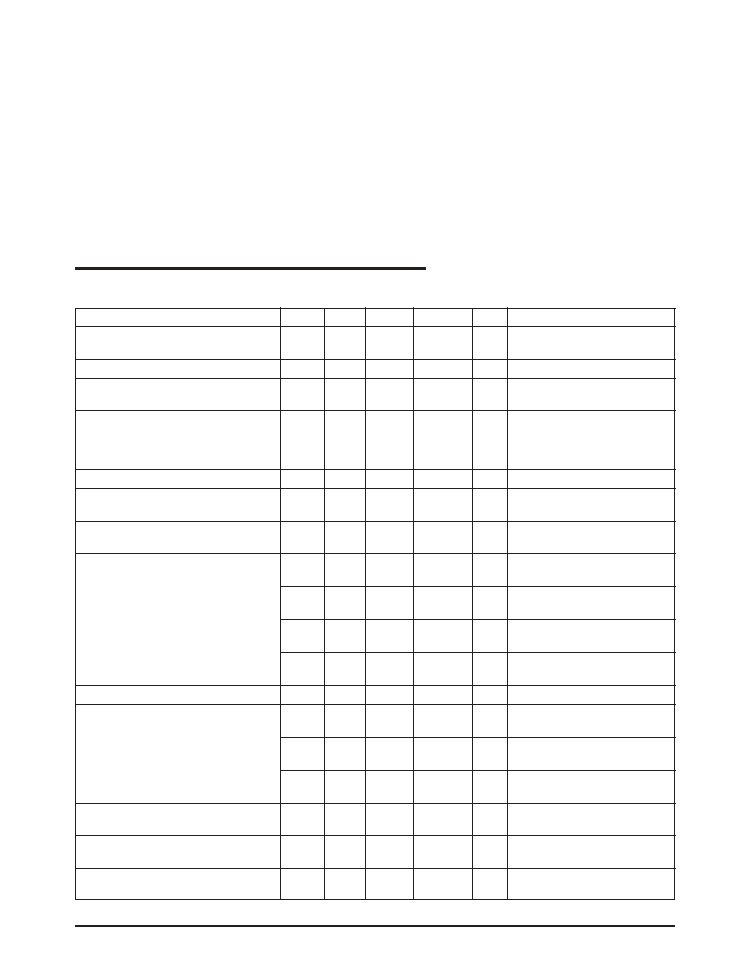
Part Number
Topmark
Temperature Range
Package Type
SP6200EM5-1.5 ................... E15 ........................ -40∞C to +125∞C ......................... 5 Pin SOT-23
SP6200EM5-1.5/TR ............. E15 ........................ -40∞C to +125∞C .
(Tape & Reel) 5 Pin SOT-23
SP6200EM5-1.8 ................... E18 ........................ -40∞C to +125∞C ......................... 5 Pin SOT-23
SP6200EM5-1.8/TR ............. E18 ........................ -40∞C to +125∞C .
(Tape & Reel) 5 Pin SOT-23
SP6200EM5-2.5 ................... E25 ........................ -40∞C to +125∞C ......................... 5 Pin SOT-23
SP6200EM5-2.5/TR ............. E25 ........................ -40∞C to +125∞C .
(Tape & Reel) 5 Pin SOT-23
SP6200EM5-2.7 ................... E27 ........................ -40∞C to +125∞C ......................... 5 Pin SOT-23
SP6200EM5-2.7/TR ............. E27 ........................ -40∞C to +125∞C .
(Tape & Reel) 5 Pin SOT-23
SP6200EM5-2.85 ................ E285 ....................... -40∞C to +125∞C ......................... 5 Pin SOT-23
SP6200EM5-2.85/TR .......... E285 ....................... -40∞C to +125∞C .
(Tape & Reel) 5 Pin SOT-23
SP6200EM5-3.0 ................... E30 ........................ -40∞C to +125∞C ......................... 5 Pin SOT-23
SP6200EM5-3.0/TR ............. E30 ........................ -40∞C to +125∞C .
(Tape & Reel) 5 Pin SOT-23
SP6200EM5-3.3 ................... E33 ........................ -40∞C to +125∞C ......................... 5 Pin SOT-23
SP6200EM5-3.3/TR ............. E33 ........................ -40∞C to +125∞C .
(Tape & Reel) 5 Pin SOT-23
SP6200EM5-3.5 ................... E35 ........................ -40∞C to +125∞C ......................... 5 Pin SOT-23
SP6200EM5-3.5/TR ............. E35 ........................ -40∞C to +125∞C .
(Tape & Reel) 5 Pin SOT-23
SP6200EM5-5.0 ................... E50 ........................ -40∞C to +125∞C ......................... 5 Pin SOT-23
SP6200EM5-5.0/TR ............. E50 ........................ -40∞C to +125∞C .
(Tape & Reel) 5 Pin SOT-23
SP6200EM5-ADJ ................ EADJ ...................... -40∞C to +125∞C ......................... 5 Pin SOT-23
SP6200EM5-ADJ/TR .......... EADJ ...................... -40∞C to +125∞C .
(Tape & Reel) 5 Pin SOT-23
SP6201EM5-1.5 ................... F15 ........................ -40∞C to +125∞C ........................ 5 Pin SOT-23
SP6201EM5-1.5/TR ............. F15 ........................ -40∞C to +125∞C . (Tape & Reel) 5 Pin SOT-23
SP6201EM5-1.8 ................... F18 ........................ -40∞C to +125∞C ........................ 5 Pin SOT-23
SP6201EM5-1.8/TR ............. F18 ........................ -40∞C to +125∞C .
(Tape & Reel) 5 Pin SOT-23
ORDERING INFORMATION
ANALOG EXCELLENCE
Corporation
Sipex Corporation
Headquarters and
Sales Office
233 South Hillview Drive
Milpitas, CA 95035
TEL: (408) 934-7500
FAX: (408) 935-7600
/TR = Tape and Reel
Pack quantity is 2500 for SOT-23 and 3,000 for DFN.
Available in lead free packaging. To order add "-L" suffix to part number.
Example: SP6200EM5-1.5/TR = standard; SP6200EM5-1.5-L/TR = lead free

17
Date:5/25/04
SP6200/6201 100/200mA CMOS LDO Regulator
© Copyright 2004 Sipex Corporation
ANALOG EXCELLENCE
Corporation
Sipex Corporation
Headquarters and
Sales Office
233 South Hillview Drive
Milpitas, CA 95035
TEL: (408) 934-7500
FAX: (408) 935-7600
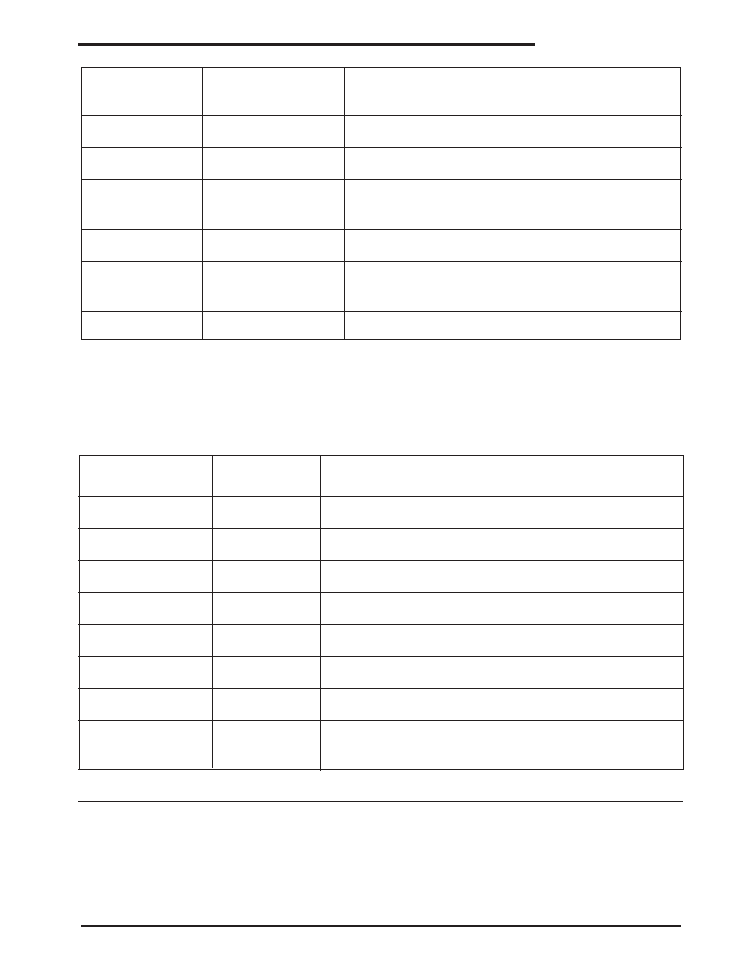
Part Number
Topmark
Temperature Range
Package Type
SP6201ER-1.8.....................ER18.........................-60∞C to +125∞C.......................... 8 Pin DFN
SP6201ER-1.8/TR...............ER18.........................-60∞C to +125∞C....
(Tape & Reel) 8 Pin DFN
SP6201EM5-2.5 ................... F25 ........................ -40∞C to +125∞C ......................... 5 Pin SOT-23
SP6201EM5-2.5/TR ............. F25 ........................ -40∞C to +125∞C .
(Tape & Reel) 5 Pin SOT-23
SP6201EM5-2.7 ................... F27 ........................ -40∞C to +125∞C ......................... 5 Pin SOT-23
SP6201EM5-2.7/TR ............. F27 ........................ -40∞C to +125∞C .
(Tape & Reel) 5 Pin SOT-23
SP6201EM5-2.85 ................ F285 ....................... -40∞C to +125∞C ......................... 5 Pin SOT-23
SP6201EM5-2.85/TR .......... F285 ....................... -40∞C to +125∞C .
(Tape & Reel) 5 Pin SOT-23
SP6201EM5-3.0 ................... F30 ........................ -40∞C to +125∞C ......................... 5 Pin SOT-23
SP6201EM5-3.0/TR ............. F30 ........................ -40∞C to +125∞C .
(Tape & Reel) 5 Pin SOT-23
SP6201EM5-3.3 ................... F33 ........................ -40∞C to +125∞C ......................... 5 Pin SOT-23
SP6201EM5-3.3/TR ............. F33 ........................ -40∞C to +125∞C .
(Tape & Reel) 5 Pin SOT-23
SP6201ER-3.3......................ER33........................-60∞C to +125∞C.......................... 8 Pin DFN
SP6201ER-3.3/TR................ER33........................-60∞C to +125∞C....
(Tape & Reel) 8 Pin DFN
SP6201EM5-3.5 ................... F35 ........................ -40∞C to +125∞C ......................... 5 Pin SOT-23
SP6201EM5-3.5/TR ............. F35 ........................ -40∞C to +125∞C .
(Tape & Reel) 5 Pin SOT-23
SP6201EM5- 5.0 .................. F50 ........................ -40∞C to +125∞C ....................... . 5 Pin SOT-23
SP6201EM5/TR ................... F50 ........................ -40∞C to +125∞C .
(Tape & Reel) 5 Pin SOT-23
SP6201EM5-ADJ ................ FADJ ...................... -40∞C to +125∞C ......................... 5 Pin SOT-23
SP6201EM5-ADJ/TR .......... FADJ ...................... -40∞C to +125∞C .
(Tape & Reel) 5 Pin SOT-23
ORDERING INFORMATION
Available in lead free packaging. To order add "-L" suffix to part number.
Example: SP6200EM5-1.5/TR = standard; SP6200EM5-1.5-L/TR = lead free
/TR = Tape and Reel
Pack quantity is 2500 for SOT-23 and 3,000 for DFN.